Home Blog Page 13

India–Japan Rare Earth Partnership: Rajasthan at the Center of a Strategic Mineral Shift

0

In a world increasingly shaped by technological competition and supply-chain security, rare earth minerals have become the new strategic currency. Now, India and Japan are exploring a powerful collaboration to jointly explore rare earth deposits in Rajasthan—an initiative that could reshape the global critical minerals landscape.

🌏 Why Rare Earth Minerals Matter More Than Ever

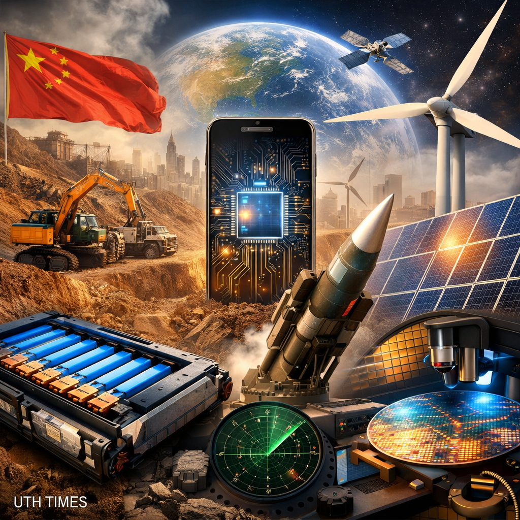
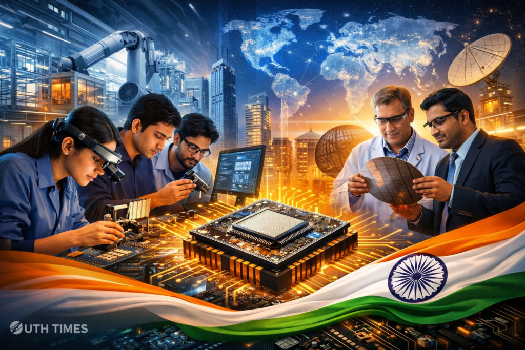
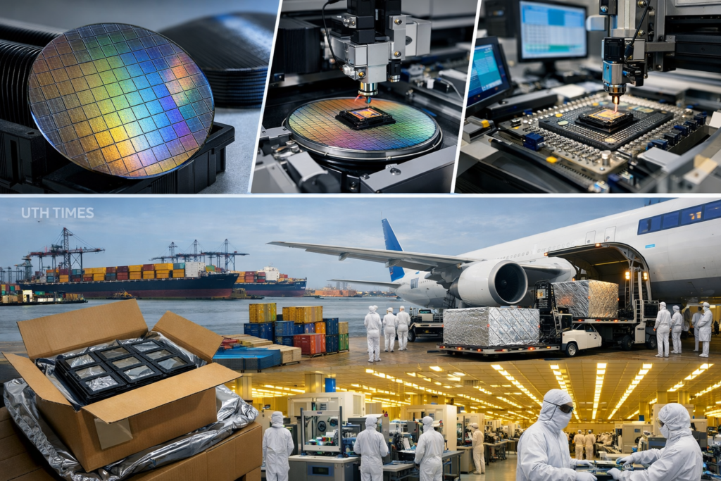
Rare earth elements (REEs) are essential for powering the technologies that define the modern world—from smartphones and electric vehicles to advanced defense systems and renewable energy infrastructure.

🔹 They are used in EV batteries, wind turbines, semiconductor chips, and missile guidance systems.

🔹 Despite their name, these elements are relatively abundant but difficult and expensive to extract and refine.

🔹 Currently, China dominates nearly 70% of global rare earth mining and around 85–90% of processing capacity, giving it immense geopolitical leverage.

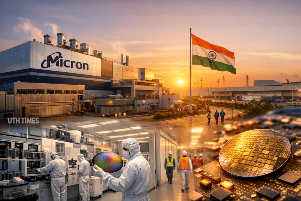
For countries like India and Japan—both major manufacturing economies—reducing dependence on Chinese supplies has become a strategic priority.

🇮🇳🇯🇵 The Rajasthan Opportunity

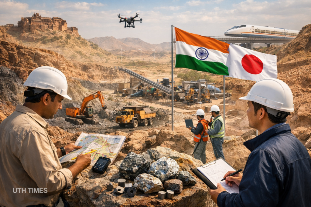
Rajasthan, known for its rich mineral reserves, has recently attracted attention for potential rare earth deposits in regions such as Barmer and Jalore. These areas may hold valuable minerals like neodymium, dysprosium, and terbium, which are critical for high-performance magnets used in EVs and electronics.

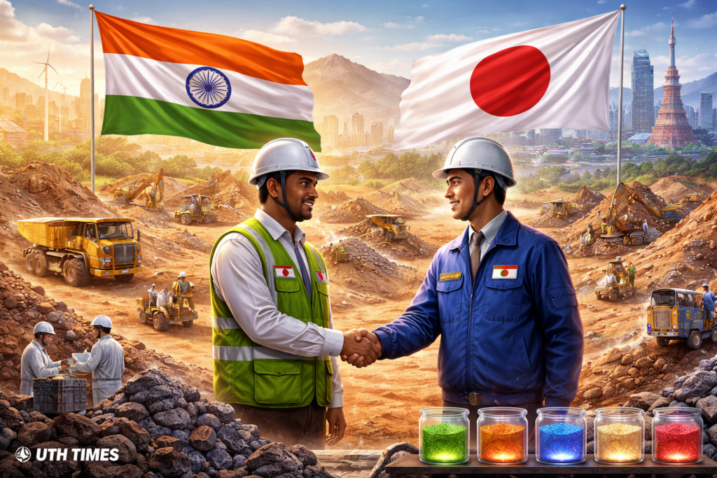
Under the proposed collaboration:

🔹 Japanese technology and expertise in rare earth processing would complement India’s mineral resources.

🔹 Joint exploration programs could involve geological surveys, advanced mapping, and pilot extraction projects.

🔹 Indian state agencies and Japanese companies may collaborate through strategic mineral partnerships.

This cooperation could significantly accelerate India’s rare earth exploration capabilities, which have historically been limited despite large geological potential.

⚙️ Strategic Impact: Beyond Mining

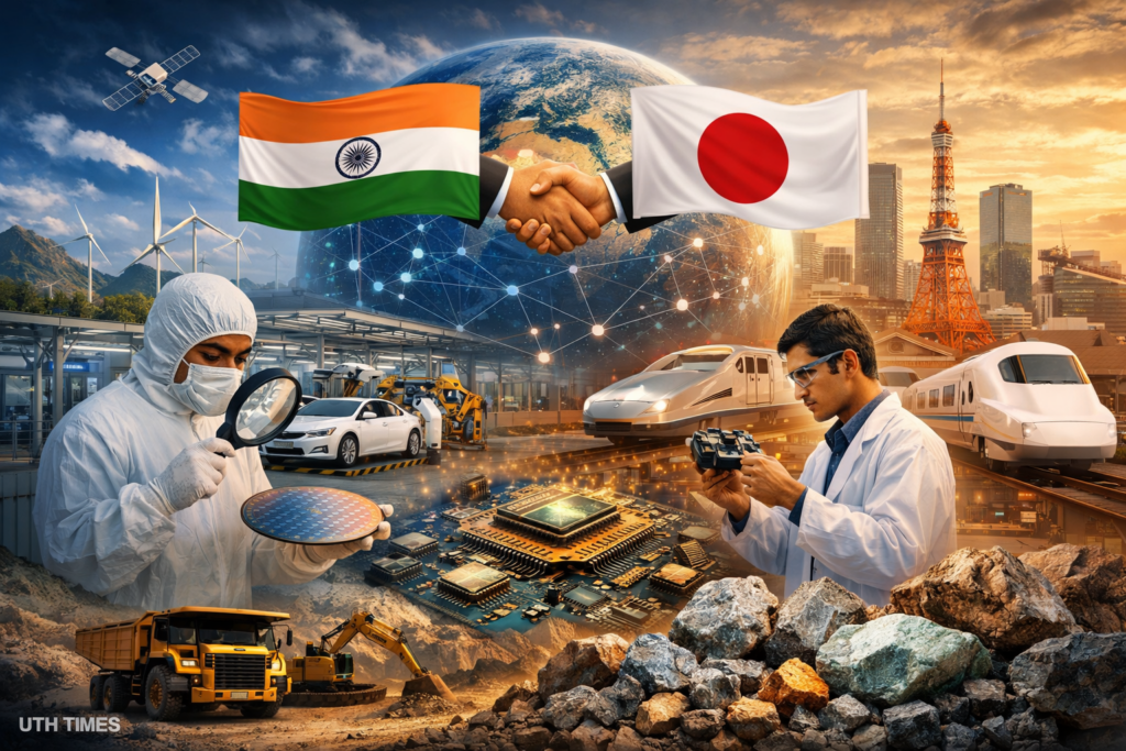
The partnership is not just about extracting minerals—it’s about building an alternative supply chain for the future economy.

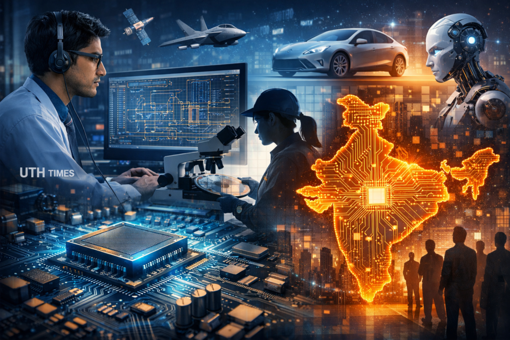
🔹 India could strengthen its domestic semiconductor, EV, and electronics manufacturing ecosystems.

🔹 Japan would gain a stable, democratic supply partner outside China.

🔹 Both nations could play a larger role in global critical mineral alliances being formed among technologically advanced economies.

Such collaborations also align with India’s broader ambitions under initiatives like Make in India and the Critical Minerals Mission, aimed at securing resources needed for next-generation industries.

🚀 A New Chapter in the Global Mineral Race

As nations scramble to secure the resources powering the green and digital revolutions, the India–Japan rare earth initiative could become a defining strategic partnership.

If successful, Rajasthan may transform from a traditional mining region into a cornerstone of the world’s next technological supply chain, positioning India as a crucial player in the global rare earth economy.

India’s Semiconductor Leap: 85,000 Chip Designers Trained in Just 4 Years

India’s ambition to become a global semiconductor powerhouse is no longer a distant policy dream—it is unfolding at remarkable speed. Under the India Semiconductor Mission (ISM), the country has successfully trained 85,000 semiconductor design engineers in just four years, achieving a target originally planned for a decade. This milestone signals a decisive shift in India’s technological trajectory, placing the nation firmly on the map of global chip innovation.

🚀 The Mission That Fast-Tracked India’s Chip Ambitions

The India Semiconductor Mission, launched in 2021, was designed to build a complete semiconductor ecosystem—from fabrication to design and research. While fabrication plants often dominate headlines, chip design talent forms the intellectual backbone of the semiconductor industry.

🔹 The mission initially aimed to train 85,000 semiconductor design engineers within 10 years.

🔹 Through accelerated academic collaborations and industry partnerships, the goal was achieved in less than half the planned time.

🔹 Engineering institutions across India integrated specialized semiconductor courses, chip architecture training, and VLSI programs into their curricula.

This rapid capacity building has created one of the largest pools of semiconductor design talent in the world, strengthening India’s position as a critical contributor to global chip development.

🧠 Why Semiconductor Design Talent Matters

Semiconductors power everything—from smartphones and electric vehicles to AI systems and defense technologies. However, design expertise is where the real value lies.

🔹 Nearly 20% of the world’s semiconductor design engineers already come from India.

🔹 Major global companies rely heavily on Indian engineers for chip architecture, verification, and system design.

🔹 Training 85,000 additional engineers significantly expands India’s capability to design next-generation chips domestically.

Instead of remaining merely a consumer of semiconductor technologies, India is now positioning itself as a creator of high-value intellectual property in chip design.

🏫 Universities, Industry & Government: A Strategic Alliance

This milestone was made possible through a three-way collaboration involving academia, government, and the semiconductor industry.

🔹 Over 300 universities and engineering institutions introduced semiconductor-focused programs.

🔹 Partnerships with global chip leaders enabled hands-on training in advanced design tools and fabrication simulations.

🔹 Government initiatives funded labs, research centers, and skill development programs dedicated to semiconductor engineering.

The result is a new generation of engineers capable of working on cutting-edge technologies like AI chips, advanced processors, and automotive semiconductors.

🌍 What This Means for India’s Tech Future

India’s early achievement of this target reflects more than just educational progress—it signals a strategic shift in technological sovereignty.

🔹 A larger talent pool attracts global semiconductor investments.

🔹 It strengthens India’s role in the global supply chain of critical technologies.

🔹 It lays the groundwork for homegrown chip startups and innovation ecosystems.

As the world races to secure semiconductor dominance, India’s rapid talent expansion could become the country’s most powerful competitive advantage.

🔮 Conclusion: The Blueprint for a Silicon Future

Training 85,000 semiconductor design engineers in four years is more than a milestone—it is a declaration that India is ready to lead in the technology that powers the modern world. With talent now scaling faster than expected, India’s semiconductor story is no longer about catching up. It is about shaping the future of global chip innovation.

The Inner Architecture of Sri Lalita Sahasranamam

The Sri Lalita Sahasranama, embedded within the Brahmanda Purana, is not merely a hymn of a thousand names — it is a metaphysical blueprint of the universe and consciousness itself. For every practitioner of Sri Vidya — whether Kādi, Hādi, or Sādi — this stotram is not optional; it is foundational.

🔱 1–3: Defining the Absolute

🕉️ The opening salutations are not ornamental — they are ontological declarations.

These names establish Lalita as the Supreme Reality: beyond duality, beyond time, beyond conceptual limitation. She is not introduced as a goddess among many — but as Para-Brahman embodied. These first invocations position Her as both the source and substratum of all existence.


✨ 4–6: Radiance & Reflection

🌟 Names 4–5 describe Her as pure effulgence — self-luminous consciousness.

🪞 Name 6 transitions into reflection — the cosmic mirror in which creation appears.

Here, theology meets metaphysics: She is both the Light and the reflective medium through which multiplicity manifests.

🌺 7–51: The Gross Form (Sthūla Rūpa)

👑 These names paint a majestic iconography — crown, eyes, smile, weapons, ornaments.

🌸 This is not mere poetic beauty; it is tantric symbolism.

Each physical attribute corresponds to a cosmic principle — the sugarcane bow (mind), flower arrows (sense faculties), noose (attachment), goad (aversion). The Divine Form becomes a philosophical diagram.

🏰 52–63: Abode & Cosmic Geography

🏔️ Names 52–54 describe Her celestial dwelling.

🌆 55–63 unfold Sripuram, the mystic city — a mandala of layered consciousness.

Sripuram is not geography; it is spiritual topology — mapping inner realization stages.

🔥 64–84: Emergence from Chidagni

🔥 Lalita arises from the Fire of Pure Consciousness (Chidagni).

⚔️ These names narrate Her divine actions — the destruction of ignorance, restoration of dharma, and revelation of esoteric truths.

Here, the Sahasranama becomes dynamic theology — divinity in motion.

🔐 85–112: Subtle Forms of Supreme Power

🕉️ 85–87: Mantra Form — She becomes sound vibration.

💗 88–89: Kāmakalā Form — the primordial creative impulse.

🐍 90–112: Kundalini Form — the coiled energy within the human spine.

These names collapse macrocosm into microcosm. The Goddess is not distant; She rises within.

Conclusion

The Sri Lalita Sahasranamam is not a list — it is a layered ascent from form to formlessness. It begins with adoration and culminates in inner awakening. To chant it is to traverse the cosmos — and ultimately, oneself.

Elon Musk’s Neuralink: Connecting the Human Brain to Machines

0

The idea of controlling computers with thoughts once belonged to science fiction. Today, Neuralink is turning that vision into reality by building implantable brain–computer interfaces (BCIs) that directly connect the human brain to digital devices. Founded in 2016 by Elon Musk and a team of scientists, the company aims to treat neurological disorders while pushing humanity toward a future where humans and artificial intelligence coexist.

The Vision Behind Neuralink

Neuralink was founded by Elon Musk and a team of neuroscientists and engineers with a long-term mission: to create a direct communication channel between the brain and computers.

Key goals include:

🔬 Restoring mobility for paralyzed patients

🧠 Treating neurological disorders like Parkinson’s and epilepsy

💻 Allowing people to control devices using only thoughts

🚀 Preparing humans for an AI-driven future

Unlike traditional medical implants, Neuralink’s technology is designed to be minimally invasive, highly precise, and scalable for mass use.

How the Neuralink Implant Works

At the heart of Neuralink’s innovation is a coin-sized implant called the Link, placed inside the skull by a specialized surgical robot.

Core technology features:

⚙️ Ultra-thin threads thinner than human hair

📡 Wireless brain signal transmission

🔋 Rechargeable battery system

🤖 Robot-assisted precision surgery

These flexible electrodes detect electrical signals from neurons and transmit them wirelessly to a computer or smartphone. The system translates neural activity into commands, allowing users to type, move cursors, or control devices using thoughts alone.

Human Trials and Breakthroughs

Neuralink entered a historic phase when it began human clinical trials in 2024.

Major milestones:

🧪 First human implant enabling thought-based cursor control

🦾 Paralyzed patients controlling computers independently

📊 Improved accuracy in decoding brain signals

🏥 FDA-approved early feasibility studies

Participants with spinal cord injuries have reportedly been able to browse the internet and play games using brain signals alone, demonstrating the real-world potential of BCIs.

Future Possibilities

Neuralink’s long-term ambitions extend far beyond medical treatment.

Potential applications include:

🚗 Controlling prosthetic limbs naturally

🎮 Immersive virtual reality experiences

🧠 Memory enhancement technologies

🤝 Human-AI integration

If successful, Neuralink could transform medicine, communication, and even human cognition itself.

The Ethical Debate

The technology also raises serious questions.

Major concerns include:

⚖️ Data privacy of brain signals

🔐 Risk of neural hacking

🧬 Long-term safety of implants

🌍 Inequality in access to enhancement technologies

Balancing innovation with ethics will determine how society adopts brain–computer interfaces.

Neuralink represents one of the boldest technological experiments of the 21st century. By bridging biology and technology, it is redefining what it means to be human — and may soon allow thoughts to become actions in the digital world.

Micron Opens $2.75B Chip Facility in Gujarat

India has entered a new era of semiconductor manufacturing as Micron Technology begins commercial production at its $2.75 billion facility in Sanand, Gujarat. The project marks one of the most significant milestones in India’s journey toward becoming a global semiconductor hub and strengthening technological self-reliance. 

India’s First Commercial-Scale Chip Facility

Micron’s Sanand plant is India’s first large-scale semiconductor production facility operating at commercial scale, representing a historic step in the country’s electronics manufacturing ambitions. 

The plant focuses on Assembly, Testing, Marking and Packaging (ATMP) — the crucial stage that converts silicon wafers into finished semiconductor products ready for global markets. 

🔹 Key Highlights

🚀 Investment: $2.75 Billion (₹22,500+ crore) 

🏭 Location: Sanand, Gujarat 

💻 Technology: DRAM and NAND memory chips 

🌍 Market: Global electronics and AI industries 

👷 Jobs: ~5,000 direct and 15,000 indirect jobs 

The facility processes advanced wafers from Micron’s global fabs and converts them into memory modules, SSDs, and semiconductor packages used in data centres, consumer electronics, and AI systems. 

How the Gujarat Plant Works

Unlike fabrication plants that create chips from raw silicon, Micron’s facility specializes in backend semiconductor manufacturing — a highly advanced process requiring precision engineering.

🔬 Production Process

⚙️ Silicon wafers arrive from global fabs 

🧪 Chips are assembled and packaged 

📊 Performance testing ensures reliability 

📦 Finished chips are exported worldwide 

The plant spans roughly 50 acres and includes large cleanroom areas, enabling high-volume semiconductor output. 

Strategic Importance for India

The launch of Micron’s facility signals India’s entry into the global semiconductor supply chain and strengthens the Make in India technology initiative. 

🌏 Strategic Impact

🛡️ Reduced dependence on imported chips

📈 Boost to India’s electronics industry

🤖 Support for AI and advanced computing

🏗️ Development of semiconductor ecosystem

Industry experts believe anchor investments like Micron will attract suppliers, research centres, and high-tech industries across Gujarat. 

A Turning Point in India’s Tech Future

Micron’s Gujarat facility is more than a factory — it represents India’s transition from a chip-consuming nation to a chip-producing power. With commercial production underway, the country is now positioned to play a meaningful role in the global semiconductor revolution.

Iran Conflict 2026: Could This Escalate Into a World War?

The Current Situation

The Middle East is facing one of the most serious military escalations in decades. The crisis intensified after joint military strikes by the United States and Israel on Iran, reportedly targeting military and strategic sites. 

These strikes triggered Iranian retaliation using missiles and drones against Israeli territory and US military bases across the Gulf region. 

The conflict has now expanded beyond Iran itself:

  • Missile strikes have spread across the Gulf region
  • Fighting has involved Iran-backed groups such as Hezbollah
  • Airspace closures and naval threats are ongoing  

This has created fears that the war could expand into a wider regional or global conflict.

Why Iran Matters Strategically

Iran is not just another regional power. Its geographic position gives it enormous influence over global trade and energy supply.

The Strait of Hormuz, near Iran’s coast, carries around 20% of the world’s oil supply, making it one of the most important trade routes on Earth. 

Disruption in this region has already caused:

  • Oil shipments halted
  • Tankers damaged
  • Ships avoiding the region
  • Rising global energy prices  

Because many countries depend on Middle Eastern energy, a prolonged conflict would have global economic consequences.

How the War Started

The tensions did not begin suddenly. They developed over decades of rivalry between:

  • Iran
  • Israel
  • The United States

Hostility increased significantly after conflicts in the Middle East since 2023, including attacks by Iran-aligned groups on US and Israeli targets. 

The current war escalated sharply after major military strikes and high-level casualties, triggering retaliation across the region. 

Could This Become World War III?

Many commentators are raising fears of a world war, but most strategic analysts say a global war is still unlikely at present.

A true world war would require major powers such as:

  • China
  • Russia
  • NATO countries

to enter the conflict directly.

At the moment:

  • The fighting is concentrated in the Middle East
  • Most countries are calling for restraint and diplomacy  
  • Military operations remain regionally focused

This makes the situation closer to a regional war with global impact, rather than a world war.

Real Risks of Escalation

Even if a world war is unlikely right now, the risks are serious.

1. Expansion to Gulf States

Iranian attacks and US bases in Gulf countries could draw more states into the conflict. 

2. Energy Crisis

Long-term disruption of oil routes could destabilize global economies. 

3. Proxy Wars

Iran-backed groups in Lebanon, Iraq, and Syria could widen the battlefield. 

4. Military Miscalculation

Accidental strikes or misinterpretations could trigger wider confrontation.

The Iran conflict is one of the most dangerous geopolitical crises of the 21st century so far.

However:

  • It is not yet a world war
  • It remains primarily a regional military conflict
  • Escalation depends on whether major powers join directly

The situation remains volatile, and the coming weeks will determine whether the conflict stabilizes or expands further.

India’s Sudarshan Chakra: The Indigenous Shield of the Skies

India is preparing to build one of the world’s most advanced aerial defence networks. Mission Sudarshan Chakra, led by DRDO, aims to create a fully indigenous multi-layered air and missile defence system by 2035, capable of protecting the nation from drones, missiles, aircraft and hypersonic threats. 

Announced as a major national security initiative, the mission represents India’s push toward complete defence self-reliance under the Atmanirbhar Bharat vision. 

What is Mission Sudarshan Chakra?

Mission Sudarshan Chakra is a nationwide AI-enabled aerial defence shield designed to protect strategic locations and population centres from modern warfare threats. 

Unlike traditional missile defence systems, Sudarshan Chakra will integrate land, sea, air, cyber and space-based defence technologies into a single networked architecture. 

Core Capabilities

🛡️ Protection against drones, cruise missiles and ballistic missiles

🛰️ Space-based threat detection using surveillance satellites

📡 Thousands of interconnected radar systems

⚡ Directed-energy weapons such as high-energy lasers

🤖 AI-based real-time threat analysis

The system is often compared to Israel’s Iron Dome, but with much wider strategic coverage and offensive capability. 

Multi-Layer Defence Architecture

Mission Sudarshan Chakra will function through overlapping defensive layers, ensuring that no aerial threat escapes interception. 

Layered Defence System

🌌 Space Layer

Satellites will detect missile launches and hostile movements in real time.

✈️ Air Surveillance Layer

Airborne early-warning aircraft and advanced radars will track targets.

📡 Ground Radar Layer

Long-range radars will monitor aerial threats across the country.

🚀 Interceptor Layer

Surface-to-air missiles and directed-energy weapons will neutralize threats.

Thousands of radars and hundreds of satellites will operate together to create a real-time national security picture. 

Key Technologies Powering the Shield

The project will integrate several advanced defence programs into one unified network.

Major Components

🚀 Project Kusha – Long-range missile defence interceptors 

⚡ Laser-based Defence Systems – Counter drone swarms 

📡 Integrated Air Defence Weapon System – Multi-target interception 

🧠 Artificial Intelligence – Predictive threat detection 

The mission will integrate Army, Navy and Air Force air defence networks into a single command system. 

Why Sudarshan Chakra Matters

Modern warfare is increasingly dominated by missiles, drones and precision strikes, making air defence a strategic necessity. 

Mission Sudarshan Chakra will ensure:

🛡️ Protection of cities and critical infrastructure

⚔️ Rapid counterstrike capability

🇮🇳 Strategic independence in defence technology

🚀 Global recognition of India’s defence innovation

Phase-wise development will continue through the next decade, with full operational capability expected by 2035, making India one of the few nations with a fully indigenous national air defence shield. 

Mission Sudarshan Chakra is not just a defence project — it is India’s blueprint for total control of its airspace in the 21st century.

L&T to Build India’s LIGO Detector in Maharashtra

0

India has taken a giant leap into the future of cosmic science. Engineering giant Larsen & Toubro (L&T) has secured a major contract to construct India’s Laser Interferometer Gravitational Wave Observatory (LIGO) in Maharashtra — a project that will allow India to “listen” to ripples in space-time created by black holes and neutron stars. 

This observatory will place India among the world’s most advanced gravitational-wave research nations.

A Mega Science Facility Rising in Maharashtra

LIGO-India will be constructed at Aundha in Hingoli district under the supervision of the Department of Atomic Energy. 

The project is part of a global scientific network studying gravitational waves — tiny distortions in space-time predicted by Einstein’s theory of relativity. 

Key Highlights

🔭 Estimated project cost: ₹2,600 crore 

🔭 Expected completion: Around 2030 

🔭 Land area: About 300 acres 

🔭 India will host one of the few LIGO detectors globally 

Once operational, the facility will function as a national research center for astrophysics and advanced physics.

L&T’s Role: Building One of the Most Precise Machines Ever

L&T’s Heavy Civil Infrastructure and Heavy Engineering divisions will jointly construct the observatory. 

Engineering Responsibilities

⚙️ Construction of ultra-precision infrastructure

⚙️ Installation of high-vacuum systems

⚙️ Manufacturing specialized beam tubes

⚙️ High-stability foundations for vibration control

The observatory will include an 8-kilometre ultra-high vacuum beam tube system, one of the most technically demanding components. 

These tubes allow laser beams to travel uninterrupted, enabling detection of cosmic signals smaller than a proton.

How India’s LIGO Will Detect the Universe

LIGO uses laser interferometers with two perpendicular arms, each about 4 km long. 

How It Works

🌌 Laser beams travel through vacuum tunnels

🌌 Mirrors reflect light back and forth

🌌 Gravitational waves stretch space itself

🌌 Tiny changes in distance are recorded

These measurements reveal violent cosmic events such as:

⭐ Black hole collisions

⭐ Neutron star mergers

⭐ Supernova explosions

Gravitational waves were first detected in 2015, revolutionizing astronomy. 

Why LIGO-India Matters Globally

India’s detector will strengthen the global gravitational-wave network and improve the accuracy of cosmic event detection. 

Scientific Impact

🚀 Better mapping of cosmic events

🚀 Improved source localization

🚀 Breakthroughs in astrophysics

🚀 New frontiers in fundamental physics

The observatory will also boost India’s reputation in frontier scientific research.

India’s Gateway to Cosmic Discovery

With L&T building one of the most sophisticated scientific instruments ever constructed in India, LIGO-India represents more than a project — it is a statement of scientific ambition.

India is no longer just observing space — it is preparing to hear the universe itself.

Light Faster Than Light: The First Real Warp Bubble

0

For decades, faster-than-light motion lived only in equations and science fiction. Now physicists have created a microscopic warp bubble that lets light outrun itself — not by breaking Einstein’s laws, but by bending space-time itself.

This is not science fiction anymore. It is a laboratory-scale distortion of reality.

Warping Space Instead of Breaking Physics

Instead of accelerating objects beyond light speed — which Einstein forbids — scientists changed the geometry of space-time itself.

Inside a microscopic region, space was compressed in front and stretched behind — the same principle behind theoretical warp drives.

🔹 Light inside the structure appeared to move faster than normal light

🔹 No physical laws were violated

🔹 No particle exceeded the speed of light locally

🔹 The effect came purely from space-time distortion

This mirrors the famous Alcubierre warp-drive concept, where a spacecraft rides a wave of space-time rather than moving through space conventionally.

The experiment produced what researchers call a metric-engineered optical medium — a material designed so precisely that it behaves like curved space-time.

In simple terms: the laboratory material became a miniature universe with its own geometry.

The Microscopic Warp Bubble

The warp bubble existed at a microscopic scale — smaller than a grain of dust — but physically real.

Scientists engineered ultra-precise materials that guided light along curved paths equivalent to a warped geometry.

🔹 Space-time curvature was simulated using metamaterials

🔹 Light paths mimicked geodesics in curved space-time

🔹 The bubble remained stable during measurement

🔹 The distortion followed Einstein’s equations

Instead of needing exotic negative energy, the experiment used structured positive-energy fields, making the model physically realistic.

This is the first time a warp-like geometry has been created in a controlled environment.

It represents a transition from theoretical relativity to experimental space-time engineering.

Why This Changes Everything

The achievement suggests warp physics may be technologically approachable — not just mathematical speculation.

🚀 Future implications include:

🔹 Laboratory tests of warp-drive metrics

🔹 New optical and gravitational technologies

🔹 Controlled manipulation of space-time geometry

🔹 Possible pathways toward interstellar propulsion

Even if starships remain centuries away, this experiment proves something extraordinary:

Space-time can be engineered.

The microscopic warp bubble does not carry spacecraft — yet. But it demonstrates a revolutionary truth:

The speed of light may be a limit for motion — but not for space itself.

Warp Drive: Bending Space for Faster-Than-Light Travel

0

For decades, faster-than-light travel belonged to science fiction. Today, scientists are designing warp drive models based on real physics, suggesting that journeys across interstellar distances might one day be possible. Instead of breaking the cosmic speed limit, warp drives aim to reshape space-time itself, allowing spacecraft to effectively outrun light without violating Einstein’s laws.

This idea is no longer pure imagination — it has become a serious topic in theoretical physics.

🚀 The Physics Behind Warp Drive

Warp drives rely on one of the strangest predictions of Einstein’s General Relativity: space-time is flexible and can stretch or compress.

🔹 A spacecraft inside a warp bubble would not move through space faster than light

🔹 Instead, space in front of the craft would contract

🔹 Space behind it would expand

🔹 The craft would ride a moving distortion of space-time

This concept was first formalized in 1994 through the Alcubierre metric, showing mathematically that warp travel is theoretically allowed.

The spacecraft would remain locally stationary while space itself moves, avoiding the relativistic limits that normally prevent faster-than-light motion.

🌀 New Warp Models Are More Realistic

Early warp drive models required more energy than exists in the observable universe, making them impractical.

Recent theoretical breakthroughs are changing that.

🔹 New designs reduce energy requirements by millions of times

🔹 Some models replace exotic matter with positive energy densities

🔹 Researchers propose stable warp bubbles that could persist longer

🔹 Mathematical simulations show warp fields may be physically consistent

Scientists are exploring shapes like soliton waves and ring-shaped energy distributions to stabilize warp fields.

These updated models suggest warp drives might be extremely difficult — but not impossible.

⚡ The Exotic Energy Problem

The biggest challenge remains energy.

Most warp drive theories require negative energy density, a strange form of energy that behaves opposite to normal matter.

🔹 Negative energy may exist in quantum vacuum fluctuations

🔹 The Casimir effect hints at small amounts of usable negative energy

🔹 No technology currently exists to generate large quantities

🔹 Energy requirements could equal planetary-scale power

Without a way to control exotic energy, warp drives remain theoretical.

🌌 Why Warp Drive Matters

Warp drive research is not just about interstellar travel.

🔹 It deepens understanding of gravity and space-time

🔹 It connects quantum physics with cosmology

🔹 It may reveal new energy technologies

🔹 It expands the limits of engineering imagination

Even if warp drives never become practical, studying them pushes physics into unexplored territory.

Warp drive research shows that faster-than-light travel may be physically possible — but technologically distant.

Humanity may still be centuries away from bending space, yet the idea that the universe allows warp travel at all may be one of the most revolutionary discoveries of modern science.